- Industry–academia powerhouse converges to fast-track India’s chip ecosystem ambitions
- Advanced packaging & power electronics emerge as next big battlegrounds
- Pilot lines at IITGN & IIT Bhubaneswar to bridge lab-to-market gap
- Global collaboration models, design-led manufacturing take centre stage
- Talent, technology, and supply chain localisation to anchor India’s chip future
NE SCIENCE & TECHNOLOGY BUREAU
GANDHINAGAR, MAR 18
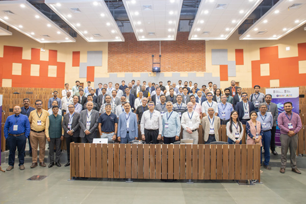
In a decisive push to position India as a global semiconductor powerhouse, the IDSPS Industry Advisory Board (IAB) Meeting at Indian Institute of Technology Gandhinagar brought together leading academia and industry voices to accelerate innovation, strengthen collaboration, and build a resilient chip ecosystem.
The high-impact deliberations saw participation from stalwarts, including Rao Tummala, CEO of IDSPS; Rajat Moona, Director, IITGN; Ashok Chandak, President of India Electronics and Semiconductor Association and SEMI; Navin Bishnoi of Marvell Technology and Chair, IAB; and Ravi Bhatkal of MacDermid and Vice Chair, IAB.
Building India’s Semiconductor Core
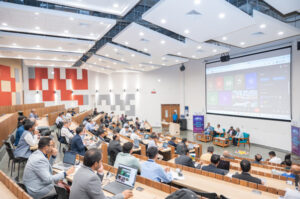
The meeting opened with a high-powered panel discussion focusing on strengthening India’s semiconductor, power electronics, and advanced manufacturing ecosystem through deep collaboration among academia, industry, and government.
“Today, we are looking at creating a strong foundation for India’s electronics and semiconductor ecosystem,” said Prof Rajat Moona, Director IITGN.
“The idea is to set up dedicated research hubs — one here and another in collaboration with the ministry, which will act as nuclei connecting various professors, institutions, and industry partners. These centres are designed to be industry-oriented, with a focus on solving real problems that matter to the market and the country.”
“Our goal is to become a multiplier — ensuring that knowledge, solutions, and innovation developed here can benefit multiple sectors and stakeholders. We are committed to creating platforms that turn ideas into actionable projects for government implementation. Initiatives in power electronics, semiconductor design, and advanced materials are key to building capabilities, fostering collaboration, and positioning India as a global technology leader,” he added.
Collaboration: The Game Changer
“Building an integrated ecosystem that connects universities, industry, and government is key for advancing electronics and semiconductor technologies,” said Prof Rao Tummala.
“Dedicated research centres and collaborative programmes will help develop skilled talent, strengthen supply chains, and position India as a global hub for next-generation technology.”
Ashok Chandak underscored the urgency of design-led growth:
“Strengthening the design-driven manufacturing ecosystem will be crucial for enhancing competitiveness and productivity across industries,” Chandak said.
“Stronger collaboration between industry, academia, and government is essential to build capabilities, encourage innovation, and respond effectively to evolving global market demands.”
Learning from global models
The panel drew insights from global best practices such as the Semiconductor Research Corporation, highlighting the need for:
• Alignment with global technology roadmaps
• Adoption of robust intellectual property frameworks
• Emphasis on peer-reviewed research as a benchmark for innovation
Deep Dive: Future Technologies
Over two days, experts engaged in detailed discussions across the semiconductor manufacturing value chain, with special focus on:
Advanced Packaging
• Design innovation and sustainable materials
• Substrate technologies and integrated opto-electronics
• Heterogeneous integration and assembly processes
Integrated Power Electronics
• Thermal management and advanced module design
• High-reliability architectures and testing frameworks
• Scalable solutions for automotive, renewable energy, and industrial sectors
These segments are expected to drive the next wave of semiconductor demand globally.
Pilot Lines: Bridging Lab to Market
A key highlight was the proposed Advanced Packaging Pilot Line at IIT Gandhinagar and Integrated Power Electronics Pilot Line at IIT Bhubaneswar, envisioned as critical infrastructure to enable prototyping, validation, and workforce training.
Shreepad Karmalkar, Director of Indian Institute of Technology Bhubaneswar, emphasised: “There is a strong need for structured engagement with industry partners and advanced technology programmes. We are committed to continuing collaborative efforts, exploring next-generation technologies, and building frameworks to support innovation, workforce development, and potential foreign direct investment opportunities.”
Roadmap for a Resilient Ecosystem
The IAB underscored key pillars for India’s semiconductor growth:
• Innovation-led ecosystem development
• Strong industry–academia translation
• Startup integration and talent pipeline creation
• Supply chain localisation and global partnerships
• Standardisation aligned with international benchmarks
The meeting concluded with a unified resolve to position IDSPS as a strategic catalyst in India’s semiconductor journey—driving self-reliance, innovation leadership, and global competitiveness.