Developed using titanium diboride-derived nanosheets, the material controls electrical flow in thin transistors with high precision while preventing energy loss
The new material is produced through a simple, scalable room‑temperature method and offers performance suited for future high‑speed, low‑power semiconductor devices
NE EDUCATION BUREAU
GANDHINAGAR, AUG 12
A few decades ago, computers capable of performing complex tasks filled entire rooms. Today, that same power fits in our pockets, built into devices lighter than a paperback. This leap has been driven by advances in semiconductor technology, where billions of tiny switches called transistors control the flow of electrical signals in everything from smartphones to satellites.
NE photo
With users demanding faster, lighter, and more energy-efficient electronics, designing materials that enable transistors to maintain their speed, efficiency, and reliability as they are scaled down has become a key challenge in semiconductor technology. In a recent breakthrough, researchers at the Indian Institute of Technology Gandhinagar (IITGN), in collaboration with Penn State University, have developed an ultra-thin insulating material that could address this challenge. Made from nanosheets of titanium diboride (TiB₂), the material offers high electrical performance and can be produced through a simple, scalable process, making it suitable for large-scale manufacturing.
“The insulating layer, or dielectric in a transistor, is more than a passive barrier between its gate that regulates current and the semiconductor channel, which allows the current to pass through,” explained Dr Kabeer Jasuja, Professor at the Department of Chemical Engineering and the Principal Investigator of the research.
“As transistors are miniaturised owing to the reduction in size of modern electronics, there is a need to design insulating materials thin enough for precise control of conductivity, yet robust enough to prevent electrical leakage that shortens the device’s lifespan.”
According to the team, unlike conventional materials, the nanosheet-based material they have discovered is capable of striking this right balance.
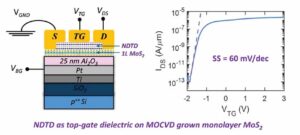
“It achieved an equivalent oxide thickness (EOT) of about two nanometres despite its physical thickness being more than fifty nanometres,” said Dr Saptarshi Das, Professor of Engineering at Penn State University, whose lab carried out the electronic studies.
NE photo
EOT is a standard way of comparing dielectric performance to silicon dioxide, the standard insulating material used in transistors. A low EOT means the dielectric can control current as effectively as a very thin layer, while the greater physical thickness provides mechanical stability and reduces leakage. “This unique combination provides the dielectric with the precision of an ultrathin insulator while maintaining the durability and leakage resistance of a thick film, a balance rarely achieved in semiconductor devices,” he added.
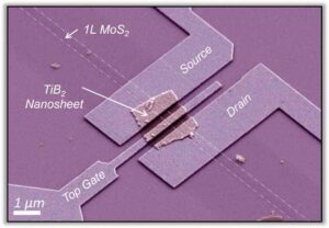
Speaking about the production of these TiB₂ nanosheets, Dr Anshul Rasyotra, first author of the study and former PhD student at IITGN, described the use of a simple, room-temperature process called dissolution–recrystallisation. As part of his IITGN Overseas Research Experience, Dr Rasyotra visited the lab of Dr Saptarshi Das at Penn State to conduct electronic studies on the nanosheets synthesised at IITGN. This method allowed them to transform bulk TiB₂ powder into sheets tens of thousands of times thinner than a human hair, without the need for high-temperature treatments or complex equipment.
Dr Jasuja elaborated, “Beyond its simplicity, the method is cost-effective, environment-friendly, and scalable. Overcoming scalability has long been a major bottleneck in translating new dielectric technologies into real-world use. Our approach could enable wider adoption among research and for industrial groups that rely on large-area, cost-effective semiconductor manufacturing.”
To evaluate the performance of the new dielectric material, the researchers tested it in transistors made with monolayer molybdenum disulfide (MoS₂), a two-dimensional semiconductor that has gained attention for its promising electrical properties. In these MoS₂-based transistors, a key performance parameter is subthreshold swing, which measures how efficiently the device can transition from the off state to the on state. A lower value means the transistor requires less voltage to switch on, making it more energy-efficient. The team achieved a subthreshold swing of 60 millivolts per decade in the transistors, which is the theoretical limit at room temperature. This means the devices can switch at the highest efficiency possible under standard conditions. They also recorded an on-off current ratio of one million at a supply voltage of just one volt, indicating precise control over current flow with minimal energy use. Furthermore, the leakage current was less than 0.0001 amperes per square centimetre, confirming the material’s strong ability to prevent unwanted energy loss. Reliability tests further revealed that the dielectric could withstand temperatures up to 125 degrees Celsius and endure over a billion switching cycles without performance degradation. Such resilience is crucial for real-world applications, where semiconductor devices are expected to operate for years under varying environmental and operational conditions.
After demonstrating high electrical efficiency and low current leakage in individual MoS₂-based transistors, the researchers tested whether the dielectric could perform just as well in a form suited for industrial fabrication. They integrated the TiB₂ layer with MoS₂ films grown using chemical vapour deposition, a technique widely used in industry to create uniform, high-quality layers over large surfaces. The results confirmed that the material maintained its strong switching performance and minimal energy loss even on these large-area films, showing its potential to move seamlessly from laboratory prototypes to manufacturing environments. Their study has been recently published in the prestigious journal ACS Nano.
According to Dr Jasuja, the work also aligns with the semiconductor industry’s ongoing “More Moore” strategy, which focuses on extending transistor miniaturisation to increase chip performance. “Our material offers a rare combination of high electrical performance, thermal stability, and manufacturing scalability,” he said.
“It is a potential candidate for integration into advanced semiconductor manufacturing, enabling smaller, faster, and more energy-efficient devices.” With its balance of properties and practical production method, the material could help sustain the pace of innovation that has defined electronics for decades.
The research team included Anshul Rasyotra, Mayukh Das, Dipanjan Sen, Zhiyu Zhang, Andrew Pannone, Chen Chen, Joan M. Redwing, Yang Yang, Prof Kabeer Jasuja, and Prof Saptarshi Das.