
- Union Minister declares AI, semiconductors and electronics manufacturing as engines of India’s next growth phase
- Semicon 2.0 to prioritise deep-tech startups, design ecosystem and equipment manufacturing backbone
- Talent gap of 20 lakh specialists opens unprecedented opportunities for India’s youth and innovation ecosystem
- Gujarat unveils Science, Technology and Innovation Policy 2026-2031 to accelerate semiconductor leadership
R MANICKAVASAGAM
GANDHINAGAR, MAR 1
SEO Keywords: Gujarat Semiconnect Conference 2026, Ashwini Vaishnaw semiconductor mission 2.0, India semiconductor design ecosystem, Gujarat Science Technology Innovation Policy 2026-2031, India semiconductor talent gap 20 lakh, AI electronics manufacturing India growth, Tata Electronics Dholera semiconductor fab.

Declaring a decisive shift in India’s technological journey, Union Electronics and IT Minister Ashwini Vaishnaw unveiled an ambitious roadmap for semiconductor leadership, asserting, “India is now learning to run from learning to walk in the field of technology.”
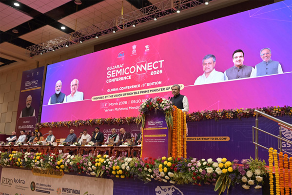
Inaugurating the Gujarat Semiconnect Conference 2026 at Mahatma Mandir in Gandhinagar, the Minister outlined the transformative vision of Semicon Mission 2.0, which will focus on strengthening design capabilities, empowering deep-tech startups and building a complete semiconductor ecosystem in India.
“AI, semiconductors and electronics manufacturing will drive India’s next growth phase,” Vaishnaw said, positioning these sectors as the backbone of the country’s future economic expansion.
Semicon 2.0 shifts focus from fabs to design, innovation and ecosystem strength
Highlighting the strategic shift under the second phase of the Semiconductor Mission, Vaishnaw said Semicon 2.0 would reverse the initial focus on manufacturing and instead prioritise building intellectual and technological capabilities.
“Semicon 2.0 will be totally the reverse of Semicon 1.0, which focused on getting manufacturing facilities in India. We got that. We have 10 plants, with the first starting commercial production yesterday. Very soon, the second plant will start commercial production,” he said.
The Minister emphasised that India’s next frontier lies in creating a globally competitive semiconductor design ecosystem capable of producing future technology leaders.
“The top priority for Semicon 2.0 will be to create a design ecosystem so that deep tech startups get the opportunity to develop the next Qualcomm, Broadcom or Nvidia,” he said.
Acknowledging the scale and complexity of the mission, he added, “It is not going to be an easy journey. It is going to be a humongous task, and we understand the complexity of it. That is why we are very realistic and pragmatic about it.”
Massive talent demand creates historic opportunity for India’s youth
Vaishnaw highlighted the extraordinary talent demand emerging in the global semiconductor industry, positioning India as a major beneficiary.
“As the semiconductor sector globally grows from 800-900 billion dollars to a trillion-dollar industry, a 20 lakh talent gap in the second phase will mean more opportunities for students,” he said.
Reaffirming the government’s commitment to skill development, he noted the rapid progress achieved under Semicon 1.0.
“In the first version, we promised that 85,000 engineers would be trained in semiconductor design in 10 years. It has been achieved in four years itself,” he said.
Expanding the talent pipeline further, the Minister announced a major increase in academic participation.
“From 350 in Semicon 1.0, we will take it to 500 universities. Every state will have several universities and colleges where students can get trained in semiconductor design, manufacturing, testing and validation, and that will create a huge, continuous stream of opportunities for youth,” he added.
Complete ecosystem—from materials to machines—key to India’s semiconductor leadership
Vaishnaw underscored the importance of building a fully integrated domestic semiconductor value chain.
He said the focus will include strengthening material supply chains, equipment manufacturing, testing and validation capabilities to ensure India’s long-term technological sovereignty.
“It is vital to have a material, machine, equipment, testing and validation ecosystem well established in the country for the foundation of the 20-year journey to be very strong,” he said.
He added that the deep-tech startup ecosystem will play a critical role in developing innovative semiconductor products designed in India and manufactured in domestic fabs.
Gujarat emerges as semiconductor powerhouse with new STI Policy 2026-2031
The conference also marked the unveiling of Gujarat’s Science, Technology and Innovation Policy 2026-2031 in the presence of Chief Minister Bhupendra Patel, reinforcing the state’s leadership in semiconductor and electronics manufacturing.
Vaishnaw described India’s semiconductor progress as historic, pointing to the launch of the Micron semiconductor facility in Sanand and ongoing fab developments across the country.
He also expressed confidence in India’s indigenous chip manufacturing future, stating that the country is on track to produce its first Made-in-India semiconductor chip by 2027.
India’s semiconductor ambitions gain momentum from Gujarat to global stage
As part of his visit, the Union Minister toured the semiconductor fabrication site of Tata Electronics at Dholera, encouraging engineers and reaffirming the government’s commitment to making India a global semiconductor hub.
With Semicon Mission 2.0 shifting focus from manufacturing to innovation, design and talent, the Gujarat Semiconnect Conference 2026 marked a defining milestone in India’s transformation from a technology consumer to a global technology creator.
Vaishnaw’s powerful assertion—“India is now learning to run from learning to walk in the field of technology”—captured the nation’s accelerating momentum toward semiconductor leadership and technological self-reliance.